Principal ASIC CAD/EDA engineer with 25+ years across physical design, CAD flow development,
PDK/library validation, physical verification, distributed EDA infrastructure, and C++/Tcl/Python/Perl
automation. Worked as both a CAD/EDA software engineer and hands-on implementation engineer, including
MPW tapeout, clean signoff, and working silicon; owned process-node/library migration, tool
interoperability, configuration/versioning, and repeatable flow bring-up.
IoT and secure embedded systems: device provisioning, cryptographic protocols, firmware/update workflows, JTAG-based validation and diagnostics
Tooling: Git, GCC, Make/CMake, Valgrind, Qt
Experience
Affinity Techworks LLC - Principal Engineer / Owner (Infrastructure, DevOps, and Applied AI) | Eugene, OR (Remote) | Sep 2025 - Present
Own infrastructure reliability and automation engagements for engineering teams, including AI-assisted workflows with operational guardrails.
Design and operationalize repeatable delivery playbooks (runbooks, automation, CI hardening) to stabilize production systems and reduce operational load.
Built and maintained an internal wiki/confluence platform with authoritative runbooks, topology/service guides, operations procedures, and software-development knowledge hubs.
Produced high-clarity system specification output for a proprietary distributed filesystem, including functional requirements, architecture, data model, protocol/security models, use cases, and test-plan mapping to accelerate implementation readiness.
Top skills: Linux, Automation, CI/CD, Docker, DevOps, Site Reliability Engineering, Technical Documentation, System Specification, Consulting
IC Manage - Senior Software Engineer | Remote (USA) | Mar 2021 - Aug 2025
Developed and optimized a high-performance C++ distributed filesystem platform for cloud-based and on-prem EDA workloads (Holodeck).
Improved performance and reliability of Holodeck EDA cloud bursting by adding I/O-driven synchronization events to support scalable cloud workflows.
Tuned storage and network I/O paths to meet EDA flow performance targets; performed low-level Linux/filesystem debugging across CI and customer environments.
Partnered with applications engineering and QA to reproduce issues, accelerate resolution, and shorten deployment turnaround; added automated diagnostics and regression coverage.
UC San Diego - OpenROAD (DARPA IDEA) - Consultant (part-time) | Remote (USA) | Mar 2019 - May 2022
Implemented and contributed to open-source physical design tooling (tapcell/welltap placement and row cutting, Tcl integration; validated with PDK/library contexts including FreePDK45 / Nangate Open Cell Library, Fujitsu 55nm / C55, ASAP7, TSMC 65LP ARM, and TSMC 16 / ARM CLN16FCLL001): github.com/The-OpenROAD-Project/tapcell
Top skills: C++, Tcl, Electronic Design Automation (EDA), Physical Design, Build Automation, GNU Make, Open Source Software, Collaboration
Stealth prototype | Wilsonville, OR (Remote) | Mar 2020 - Feb 2021
Built a GPS position-aware video-analytics prototype, extracting forencis evidence and kinematics from CCTV dashcam, drone footage. https://github.com/dmitrymironov/SpaceHammer.
Top skills: C++, Python, Data Processing, Automation, Git, Software Prototyping, Garmin, GPS, Tapo, ZoneMinder
Siemens EDA (Mentor Graphics) - Contractor | Wilsonville, OR / Fremont, CA | Jun 2018 - Mar 2020
Delivered infrastructure, agent, and server improvements: build/release automation, regression environment work, and rollout of bug tracking.
Maintained and extended AMS/Nexys/FTDI/VIP modules; created new agents (ARM demo) and improved embedded performance by rewriting critical paths in C.
Designed and implemented a Rendezvous server supporting ARM demo workflows; provided peripheral support for MindSphere and Mbed Cloud.
Integrated cloud IoT onboarding (AWS IoT, Azure IoT) into demo/provisioning workflows and optimized ARM mbed client integration for embedded agents.
Top skills: C++, Embedded Systems, ARM, Internet of Things (IoT), Amazon Web Services (AWS), Microsoft Azure, Linux, Networking, Automation
Siemens EDA (Mentor Graphics) - Design for Security (System Level Engineering) - Contractor | Wilsonville, OR | Dec 2011 - Sep 2012
Delivered end-to-end physical implementation and tapeout for a security testchip SoC using TSMC CL018G / 0.18um MPW backend flows and tcb018gbwp7t standard-cell/library setup, including power grid/filler integration, hard-IP GDS "ghost" blocks, P&R (Innovus/ICC2), STA/SDF, and Calibre DRC/LVS; supported TSMC MPW packaging resulting in functional silicon.
Built secure provisioning and device-authentication protocols across x86/ARM agents, JTAG-based exchange with secure IP, and a REST API backend; converted specs into UML sequence diagrams for implementation traceability.
Drove system bring-up and debug on FPGA prototypes and silicon using C/C++ and Tcl: JTAG/TAP automation, UART/SPI validation, and Questa DPI simulations for hardware-software verification.
Built FPGA/JTAG debug tooling and in-house CAD utilities in C++/Tcl to accelerate bring-up and validation.
Nangate A/S - Head of Representative Office | Moscow, Russia | Dec 2005 - Nov 2011
Established and led Russian R&D for automated standard-cell library generation/validation, scaling the team to 30+ engineers by 2011.
Built Xvalid standard-cell library semantic validation suite and parsing pipeline (C++/Lex/Yacc/Boost.Polygon, SWIG/Tcl) to cross-check Liberty/LEF/GDSII/Verilog/SPICE views and enforce pin/area/geometry consistency; validated libraries with Cadence and ICC2 flows.
Supported customer-facing library delivery and acceptance, balancing engineering execution with partner coordination.
Top skills: Standard Cell Libraries, Electronic Design Automation (EDA), VLSI, ASIC, C++, Tcl, Lex/Yacc, Regression Testing, Computational Geometry
Selected Consulting Engagements
Supported 30+ client and partner organizations across consulting, EDA, infrastructure, and product-development work.
Runtime Design Automation (RTDA) / Runtime Inc. (2013-2015): built FlowTracer grid-based design-space-exploration pipelines; composed distributed EDA flows and extracted QoR metrics from tool logs (WNS/TNS, congestion, routing, power, HPWL).
Nangate (Sep-Oct 2015): fixed library acceptance-test failures in Xvalid (GDS ingestion, geometry/text-label and pin checks).
Kerrisdale Capital (Mar 2016): authored biometric fingerprint sensor research and forward-looking market analysis.
Silvaco (Oct 2017): stabilized and benchmarked Fabrix flows (build/config management, reference P&R runs, 3-layer support, partitioned modes), including X-FAB XC06 5.0V Digital Core Library variants.
Earlier Experience (Select)
Synopsys / Gambit Automated Design (1993-1999): Joined a P&R startup as an intern while pursuing an Engineer Diploma (M.S.-equivalent) in semiconductor CAD engineering at MIET (completed in 1997), combining education and professional engineering work; grew into a Principal Engineer role contributing high-performance CAD C++ code and architecture across placement, floorplanning, legalization, CTS/ECO, and timing-driven optimization, with team execution contributing to the company’s acquisition by Synopsys.
Arcadia Design Systems (1999-2000): Delivered major Mustang datapath placer improvements, including macro pin-to-bus alignment techniques that significantly reduced routing violations/shorts and improved overall placement quality.
Tera Systems (2000-2001): built datapath block placement for rapid virtual prototyping, using RTL-to-gates synthesis, Design Compiler, PrimeTime STA feedback, SDC timing budgets, fast routing approximation, and Visual C++/MFC GUI.
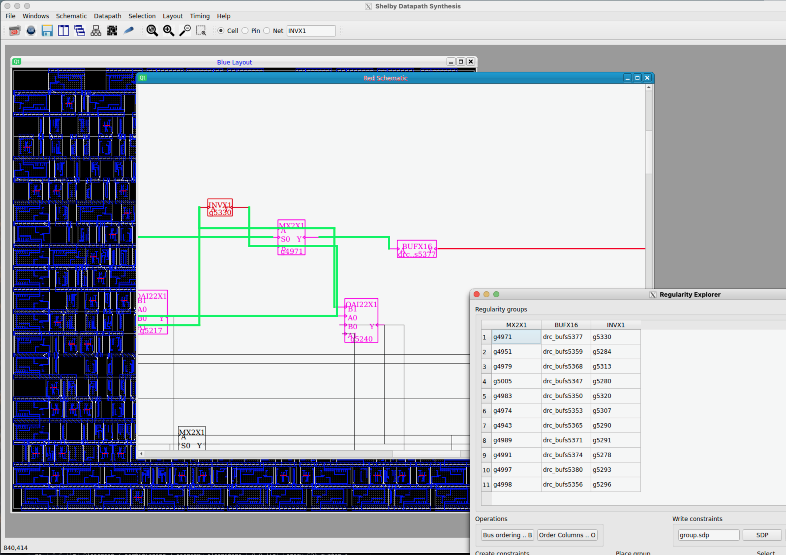
Shelby Datapath Synthesis (independent Novorado product prototype): built a datapath regularity extraction and placement tool with Qt GUI, LEF/DEF/GDS/Liberty/Verilog/SPICE parsing, regularity-group detection, structured placement exploration, and constraint generation for datapath-oriented physical design.
Shelby datapath extractor/placer. Open full size.
AmmoCore Technology (2001-2003): refactored and optimized Fabrix detailed placement for a distributed HPC/grid P&R system; configured and supported reference/regression flows across technology/library stacks including Centillium t013s7ml/t013s7ml_lv 0.13um, Toshiba tc260c/tc260c_hifn/toshiba_high_speed 0.15um, TSMC 0.25um Artisan libraries, NEC CB11/CB12/CB130M/ned3, Fujitsu CS81Z/CS91_ARMCORE/CS91_Twincle/SC82, Hitachi 76C035, Broadcom internal processes, and Mitsubishi processes.
Silicon Valley Research (Silvaco) (2003): CAD/EDA algorithms and UI; cross-platform C/C++ porting (Sun/HP-UX).
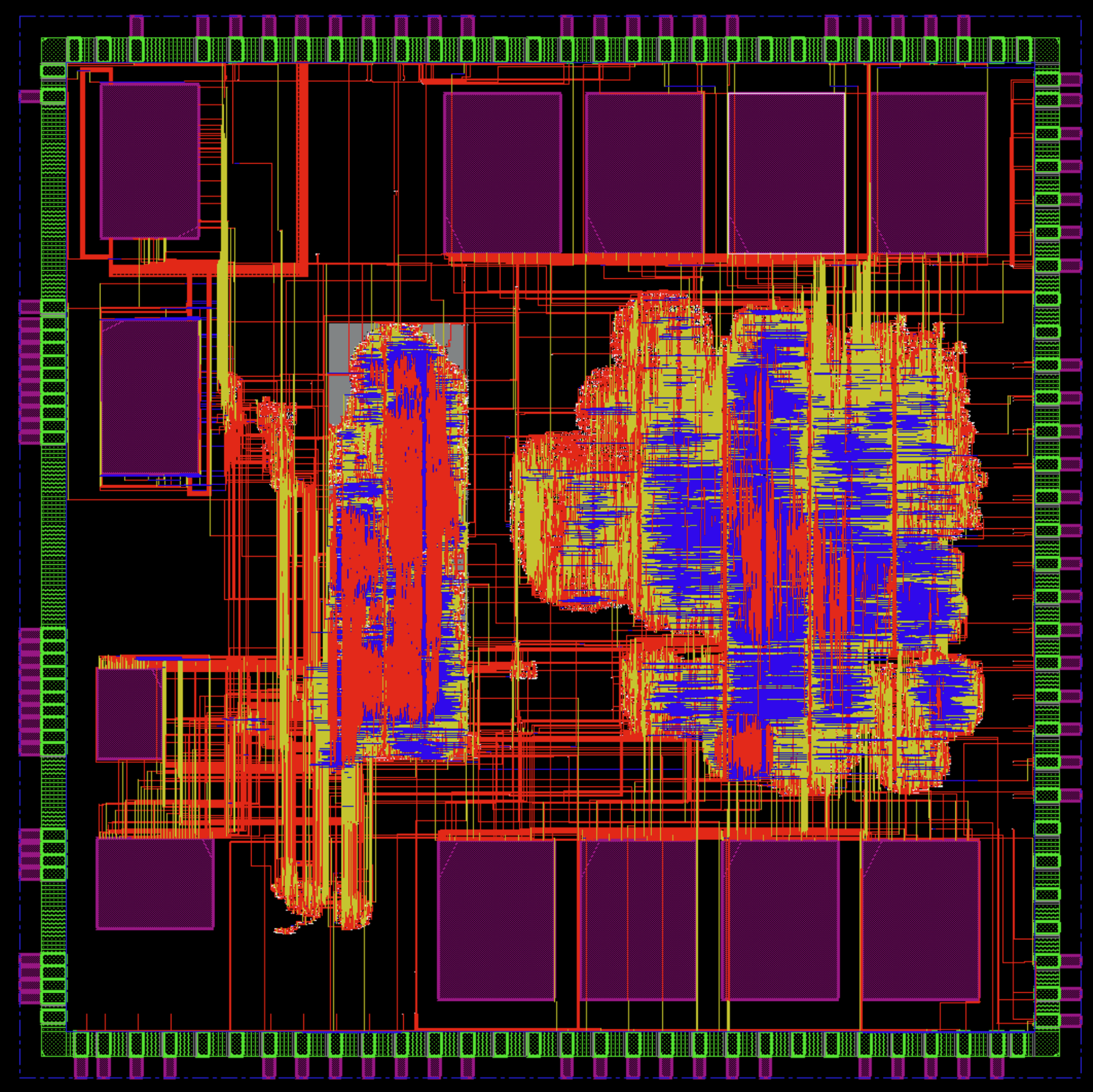
Crypto processor physical layout. Open full size.
Charles Schwab (CyberTrader platform) (2003-2005): software QA project management in finance (via Allied Testing), including test strategy, documentation, and transaction-validation workflows with dev/ops coordination.
AMCAD Engineering (2013-2014): served as General Director, representing the company to the Space Cluster Administration and leading government relations and commercial operations; defined a small-scale PCB fab pilot stack (Mega-UK/FTX, Bungard, Limata LDI, AccurateCNC, Fisnar, Dynamask/Laminar) alongside RF/microwave and satellite-communications initiatives.
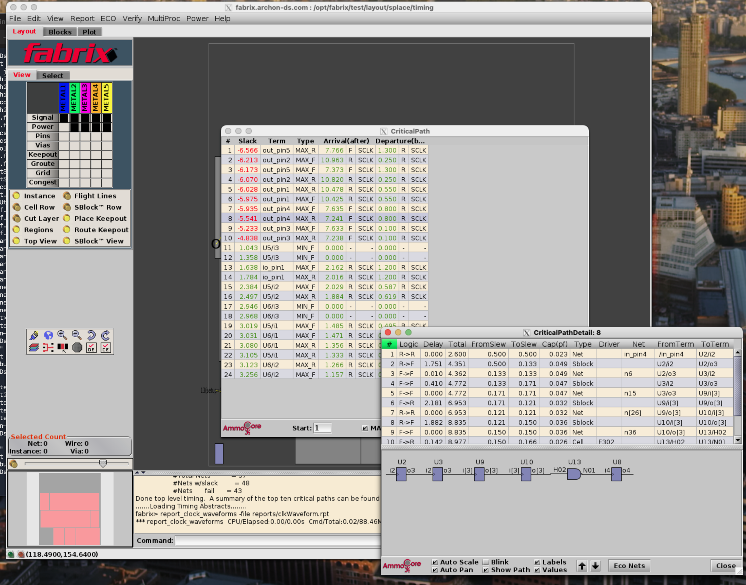
Archon Design Solutions - Contractor (C++/Tcl) | San Jose, CA (Remote) | Dec 2011 - Nov 2017: modernized and stabilized Fabrix RTL-to-GDSII flows (portability, profiling, concurrency, build/regression reliability, and format/toolchain upgrades), including X-FAB XT018 / xt018 library support and LEF/DEF/Liberty/GDS/CDL/Verilog data migration.
Fabrix RTL-to-GDSII flow screenshot. Click to open full size.
OpenSource Projects
usbpark: Open-sourced parking-assist firmware, UI and PCB design package for long-term maintainability of deployed systems; github.com/dmitrymironov/usbpark-code.
rigol2ltspice: Utility to convert Rigol waveform captures into LTspice-compatible input data for simulation workflows; github.com/dmitrymironov/rigol2ltspice.
Education
Moscow Institute of Electronic Technology (MIET): Engineer Diploma АВС 0380104 | 1992 - 1997
MS CS/EE in Semiconductor physics, IC CAD algorithms and methods, Verification Authority: Foundation for International Services, Inc. (FIS), Evaluation: 81933/WEJ
Thesis: Optimizing standard-cell layouts using ECO change-order techniques, including cell orientations, structural pin alignment, and force-directed improvements, followed by optimal placement legalization. After graduation, entered a Ph.D. program in transistor device engineering at the Lukin Scientific Research Institute of Physical Problems (NIIFP), Zelenograd; the program was not completed after receiving an offer and relocating abroad.
Certifications
Machine Learning in Production: Sep 2025 | Credential ID: R1I1SAPQQCNV
Deep Learning Specialization: Dec 2020 | Credential ID: LZRWTYZ7BZJ2
AWS Fundamentals Specialization: Oct 2020 | Credential ID: KRJEDDPY6LS2
Machine Learning: Oct 2020 | Credential ID: 89YZ8K8MNHVC